On May 15, 2025, MasterPlus Optics & Photonics students from TU/e, TU Delft, and the University of Twente came together for an inspiring visit to ASML, one of the world’s leading technology companies in the semiconductor industry. Headquartered in Eindhoven, the Netherlands, ASML is renowned for its cutting-edge photolithography systems and plays a crucial role in global chip manufacturing—deeply connected to the fields of optics and photonics.
The visit was part of the High-Tech Exchange program organized by the Photonics Society Eindhoven, offering students a unique opportunity to explore real-world applications of photonics and connect with peers and professionals.
Insights from ASML Experts
After a warm welcome and coffee, students attended a presentation titled “ASML in a nutshell,” followed by engaging pitches from five ASML experts—each working in different departments and on various photonics-related technologies. From cleanroom operations to EUV lithography, students got a behind-the-scenes look at how ASML uses tin droplets and laser pulses to generate extreme ultraviolet light for chip production.
One expert shared valuable insights into the transition from PhD research to industry, highlighting how technical challenges are approached differently in a corporate setting. Another explained the research and innovation funnel, showing how ASML transforms research and innovation into the next generation of lithography machines
Networking and Career Exploration
During the Q&A and networking session, students had the chance to ask questions about career paths, work culture, and the diverse roles within ASML. The informal lunch that followed allowed for further conversations—not only with ASML professionals but also among students from different universities.
Learning from Each Other
In the afternoon, students visited the ASML Experience Center, where they learned about the evolution of lithography machines and chip-making processes. This was followed by two poster sessions, where students presented and discussed their research projects in integrated photonics. These sessions fostered peer-to-peer learning and sparked conversations about PhD opportunities and academic collaboration.
A Truly International Exchange
The event was part of a three-day High-Tech Exchange, bringing together international students and PhD candidates in optics and photonics. It offered MasterPlus students a chance to connect with a broader community, share experiences, and build networks across borders.
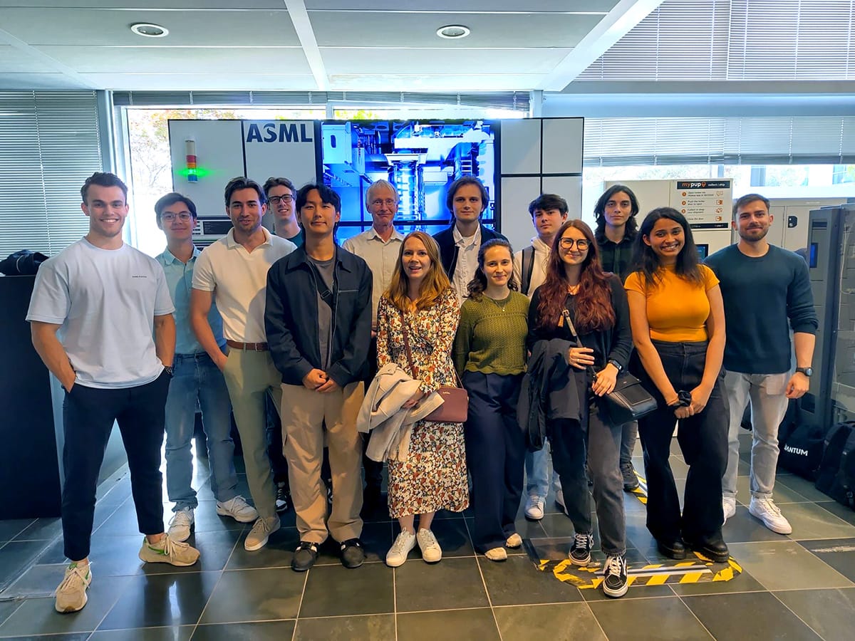
The day concluded with drinks, a group photo, and plenty of new connections—making it a memorable experience for everyone involved.